
1
P/N:PM1171
REV. 1.0, FEB. 27, 2006
MX29LA129M H/L
128M-BIT SINGLE VOLTAGE 3V ONLY
UNIFORM SECTOR FLASH MEMORY
FEATURES
GENERAL FEATURES
∑ Single Power Supply Operation
- 2.7 to 3.6 volt for read, erase, and program opera-
tions
∑ Configuration
- 16,777,216 x 8 / 8,388,608 x 16 switchable
∑ Sector structure
- 64KB(32KW) x 256
∑ Latch-up protected to 250mA from -1V to VCC + 1V
∑ Low VCC write inhibit is equal to or less than 1.5V
∑ Compatible with JEDEC standard
- Pin-out and software compatible to single power sup-
ply Flash
PERFORMANCE
∑ High Performance
- Fast access time: 90R/100ns
- Page read time: 25ns
- Sector erase time: 0.5s (typ.)
- 4 word/8 byte page read buffer
- 16 word/ 32 byte write buffer: reduces programming
time for multiple-word/byte updates
∑ Low Power Consumption
- Active read current: 18mA(typ.)
- Active write current: 20mA(typ.)
- Standby current: 20uA(typ.)
∑ Minimum 100,000 erase/program cycle
∑ 20-years data retention
SOFTWARE FEATURES
∑ Support Common Flash Interface (CFI)
- Flash device parameters stored on the device and
provide the host system to access.
∑ Program Suspend/Program Resume
- Suspend program operation to read other sectors
∑ Erase Suspend/ Erase Resume
- Suspends sector erase operation to read data/pro-
gram other sectors
∑ Status Reply
- Data# polling & Toggle bits provide detection of pro-
gram and erase operation completion
HARDWARE FEATURES
∑ Ready/Busy (RY/BY#) Output
- Provides a hardware method of detecting program
and erase operation completion
∑ Hardware Reset (RESET#) Input
- Provides a hardware method to reset the internal
state machine to read mode
∑ WP#/ACC input
- Write protect (WP#) function allows protection of all
sectors, regardless of sector protection settings
- ACC (high voltage) accelerates programming time
for higher throughput during system
SECURITY
∑ Sector Protection/Chip Unprotect
- Provides sector group protect function to prevent pro-
gram or erase operation in the protected sector group
- Provides chip unprotect function to allow code
changes
- Provides temporary sector group unprotect function
for code changes in previously protected sector groups
∑ Sector Permanent Lock
- A unique lock bit feature allows the content to be
permanently locked
(Please contact Macronix sales for specific infor-
mation regarding this permanent lock feature)
∑ Secured Silicon Sector
- Provides a 128-word OTP area for permanent, se-
cure identification
- Can be programmed and locked at factory or by cus-
tomer
PACKAGE
∑ 56-pin TSOP
GENERAL DESCRIPTION
The MX29LA129M H/L is a 128-mega bit Flash memory
organized as 16M bytes of 8 bits or 8M words of 16 bits.
MXIC's Flash memories offer the most cost-effective and
reliable read/write non-volatile random access memory.
The MX29LA129M H/L is packaged in 56-pin TSOP. It is
designed to be reprogrammed and erased in system or in
standard EPROM programmers.
The standard MX29LA129M H/L offers access time as
fast as 90ns, allowing operation of high-speed micropro-
cessors without wait states. To eliminate bus conten-
tion, the MX29LA129M H/L has separate chip enable
(CEx) and output enable (OE#) controls.
MXIC's Flash memories augment EPROM functionality

2
P/N:PM1171
REV. 1.0, FEB. 27, 2006
MX29LA129M H/L
with in-circuit electrical erasure and programming. The
MX29LA129M H/L uses a command register to manage
this functionality.
MXIC Flash technology reliably stores memory contents
even after 100,000 erase and program cycles. The MXIC
cell is designed to optimize the erase and program
mechanisms. In addition, the combination of advanced
tunnel oxide processing and low internal electric fields
for erase and programming operations produces reliable
cycling. The MX29LA129M H/L uses a 2.7V to 3.6V
VCC supply to perform the High Reliability Erase and
auto Program/Erase algorithms.
The highest degree of latch-up protection is achieved
with MXIC's proprietary non-epi process. Latch-up pro-
tection is proved for stresses up to 100 milliamperes on
address and data pin from -1V to VCC + 1V.
AUTOMATIC PROGRAMMING
The MX29LA129M H/L is byte/word/page programmable
using the Automatic Programming algorithm. The Auto-
matic Programming algorithm makes the external sys-
tem do not need to have time out sequence nor to verify
the data programmed.
AUTOMATIC PROGRAMMING ALGORITHM
MXIC's Automatic Programming algorithm require the user
to only write program set-up commands (including 2 un-
lock write cycle and A0H) and a program command (pro-
gram data and address). The device automatically times
the programming pulse width, provides the program veri-
fication, and counts the number of sequences. A status
bit similar to DATA# polling and a status bit toggling be-
tween consecutive read cycles, provide feedback to the
user as to the status of the programming operation.
AUTOMATIC CHIP ERASE
The entire chip is bulk erased using 50 ms erase pulses
according to MXIC's Automatic Chip Erase algorithm. The
Automatic Erase algorithm automatically programs the
entire array prior to electrical erase. The timing and veri-
fication of electrical erase are controlled internally within
the device.
AUTOMATIC SECTOR ERASE
The MX29LA129M H/L is sector(s) erasable using MXIC's
Auto Sector Erase algorithm. Sector erase modes allow
sectors of the array to be erased in one erase cycle. The
Automatic Sector Erase algorithm automatically programs
the specified sector(s) prior to electrical erase. The tim-
ing and verification of electrical erase are controlled inter-
nally within the device.
AUTOMATIC ERASE ALGORITHM
MXIC's Automatic Erase algorithm requires the user to
write commands to the command register using stan-
dard microprocessor write timings. The device will auto-
matically pre-program and verify the entire array. Then
the device automatically times the erase pulse width,
provides the erase verification, and counts the number
of sequences. A status bit toggling between consecu-
tive read cycles provides feedback to the user as to the
status of the programming operation.
Register contents serve as inputs to an internal state-
machine which controls the erase and programming cir-
cuitry. During write cycles, the command register inter-
nally latches address and data needed for the program-
ming and erase operations. During a system write cycle,
addresses are latched on the falling edge, and data are
latched on the rising edge of WE# .
MXIC's Flash technology combines years of EPROM
experience to produce the highest levels of quality, reli-
ability, and cost effectiveness. The MX29LA129M H/L
electrically erases all bits simultaneously using Fowler-
Nordheim tunneling. The bytes are programmed by us-
ing the EPROM programming mechanism of hot elec-
tron injection.
During a program cycle, the state-machine will control
the program sequences and command register will not
respond to any command set. During a Sector Erase
cycle, the command register will only respond to Erase
Suspend command. After Erase Suspend is completed,
the device stays in read mode. After the state machine
has completed its task, it will allow the command regis-
ter to respond to its full command set.
3
P/N:PM1171
REV. 1.0, FEB. 27, 2006
MX29LA129M H/L
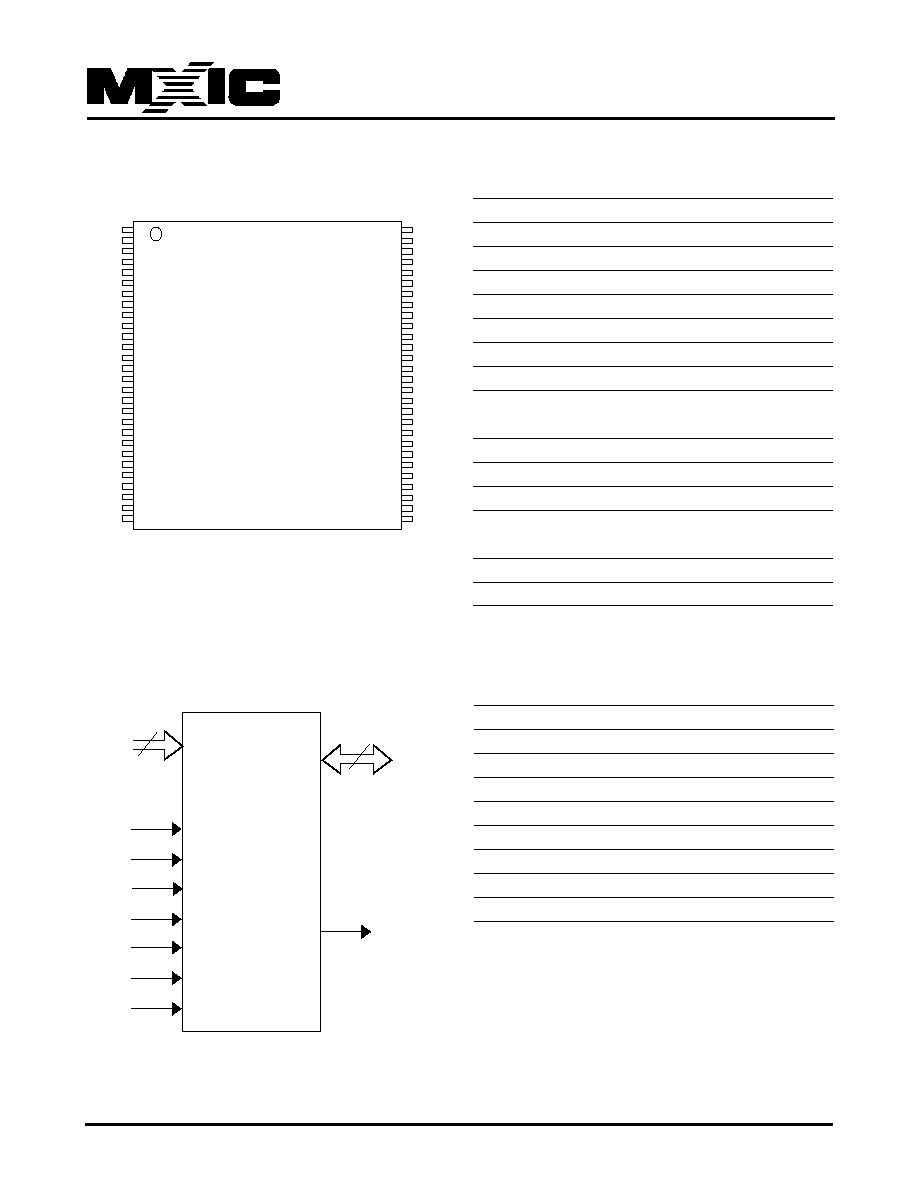
PIN CONFIGURATION
56 TSOP
SYMBOL
PIN NAME
A0
Byte-Select Address
A1~A23
Address Input
Q0~Q15
Data Inputs/Outputs
CE0~CE2
Chip Enable Input
WE#
Write Enable Input
OE#
Output Enable Input
RESET#
Hardware Reset Pin, Active Low
WP#/ACC Hardware Write Protect/Programming
Acceleration input
RY/BY#
Read/Busy Output
BYTE#
Selects 8 bit or 16 bit mode
VCC
+3.0V single power supply
VI/O
Output Buffer Power (2.7V~3.6V this
input should be tied directly to VCC )
GND
Device Ground
NC
Pin Not Connected Internally
PIN DESCRIPTION
LOGIC SYMBOL
Chip Enable Truth Table
CE2
CE1
CE0
DEVICE
VIL
VIL
VIL
Enabled
VIL
VIL
VIH
Disabled
VIL
VIH
VIL
Disabled
VIL
VIH
VIH
Disabled
VIH
VIL
VIL
Enabled
VIH
VIL
VIH
Enabled
VIH
VIH
VIL
Enabled
VIH
VIH
VIH
Disabled
Note: For Single-chip applications, CE2 and CE1 can be
strapped to GND.
16 or 8
Q0-Q15
RY/BY#
A0-A23
CEx
OE#
WE#
RESET#
WP#/ACC
BYTE#
VI/O
24
A22
CE1
A21
A20
A19
A18
A17
A16
VCC
A15
A14
A13
A12
CE0
WP#/ACC
RESET#
A11
A10
A9
A8
GND
A7
A6
A5
A4
A3
A2
A1
1
2
3
4
5
6
7
8
9
10
11
12
13
14
15
16
17
18
19
20
21
22
23
24
25
26
27
28
NC
WE#
OE#
RY/BY#
Q15
Q7
Q14
Q6
GND
Q13
Q5
Q12
Q4
VI/O
GND
Q11
Q3
Q10
Q2
VCC
Q9
Q1
Q8
Q0
A0
BYTE#
A23
CE2
56
55
54
53
52
51
50
49
48
47
46
45
44
43
42
41
40
39
38
37
36
35
34
33
32
31
30
29

